Introduction
We’re on the verge of being able to describe all the main components of real processors! Huzzah, we are well on our way to getting real software up and running! Get excited!
As one final preparation step, we want to do two things - set the historical scene for what problem the design of the first processors was solving. We also want to explore a less-common but very-useful digital device called a “tri-state” buffer that will be key to our processor design function.
Some History
Way back in the day, if you had a lot of math to do, you would hire a human computer - literally, a person whose job it was to do computations. You gave them a set of instructions as to what math to do, and they came back with a set of numbers. Not a glamorous job, but it did pay the bills. If you had big calculations to do, you’d hire lots of them and find ways to divide the work. If you wanted to ensure accuracy, you’d hire twice as many as needed and have them both independently solve the same problem (and check the results).
Obviously, there are some big limitations to this system. Humans make mistakes, grueling hours of arithmetic isn’t exactly the most fun way to spend your work day, and there’s only so fast that a human can do math. You can’t take a big problem and subdivide it efficiently between a million people, as the complexity of re-combining the results starts to outweigh the benefits of doing work in parallel. Due to these limitations, and the ever-increasing scope of work, there was a need to expand the computing capability of the scientific community in general.
Toward the end of World War I and into World War II, there was an expanding notion of using machines to do rapid computation. The proximity to war-time meant a lot of the computation applications were, well, war-driven. Cryptography, attempting to break cryptography, calculating artillery trajectories, analyzing the feasibility of an atomic bomb…. Some simply calculated differential equations, but again the majority of the funding was pushed toward war-time effort.
These machines were quite large. Remember that the transistor had not yet been invented. The logic gates we have studied were conceptually still in use, but to implement them engineers had to use vacuum tubes or electro-mechanical switches. Additionally, the first machines were effectively hard-coded to do one single job. The government would come in and say “Johnson! We need a machine to help shoot shells at the enemy better! Here’s the equations, figure it out!” And then Johnson would go wire up one machine to do the job, and come back with an answer, and then the machine would be useless. Well, not entirely useless. But still, to do a different job (or even just tweak the equations), you had to spend lots of time re-designing parts of the circuitry, have technicians come in and physically re-wire the thing, test it all out, and hope you didn’t make any mistakes in the process.
Given the need for speed in reprogramming, a group of engineers set out to design a machine which was much more easily reprogrammable. The quest was for a “general purpose” computer, which could do arbitrary computations as needed, and did not take a team of technicians to re-wire every time computational problem changed.

Alan Turing provided a key portion of the theoretical background for the general purpose computer. The “Turing Machine” is a formal mathematical description of what sorts of devices can perform general computation. His papers show both what sorts of problems are “computable” (ie solved with an algorithm, acting only with numbers, math, and logic), and what criteria a machine must have to solve an arbitrary problem. This ability to solve an arbitrary problem is what makes a computer “general-purpose”.
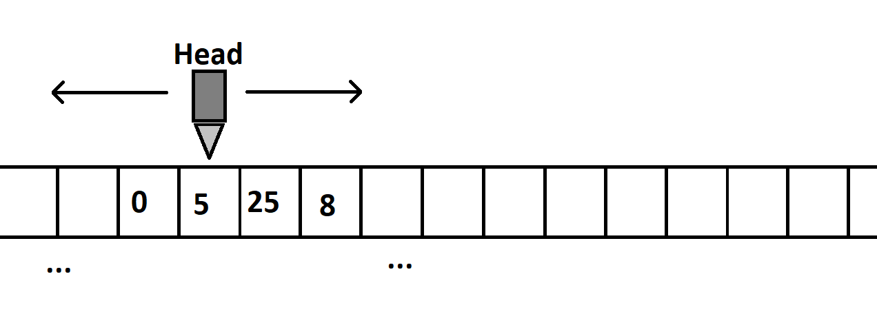
The classic demonstration of a simple Turing Machine involves a very large piece of magnetic tape, and a Head - a device capable of moving along the tape, with the ability to read and write information from defined locations on the tape. The simple implementation is still problem specific - the instructions for how it reads, writes, and moves are hard-coded into the specific Turing Machine. Turing himself showed the possibility of a “Universal Turing Machine”, which has a single programmed behavior to read the actual instructions from the tape itself. Therefor, the machine did not have to be changed, only the instructions stored in the tape. This is the basis of the “stored program” concept.
As-described, the actual Turing Machine is not particularly practical to build. It presumes a mechanical analogy, which fundamentally limits speed and size. Still, the theoretical background was required to provide the constraints on how to hook up an electronic circuit such that the end result would ultimately solve the problem. Turing effectively provided the input constraints, and pass-fail criteria for the stored-program, general-purpose computer.
John Von Neumann was another other major player in the early development of these stored-program computers. He is usually credited for leading the charge of transforming Turing’s theoretical work into a practical implementation of a general-purpose computer. He was highly involved in the design and development of EDVAC and later ENIAC, two of the first useful stored-program machines. The design we are about to study is the design he is largely credited for inventing.
As a side note, both Turing and Von Neumann were crazy smart people, with scientific contributions well beyond the processor architecture we are studying.. Given all they did, its almost a disservice to think of them as the founders of the modern computer, as their influence in the scientific community was much broader.
Stored Program
The “stored program” is really the key to unlocking programming efficiency and making computers general-purpose. A stored program is exactly what it sounds like. The program, or set of instructions for operation, is stored in a memory bank somewhere.
This memory bank has to be purpose-designed to be easily manipulated. Data must be stored and retrieved at will, usually without direct human intervention (ie, no technician coming by to move wires).
A stored program machine has to have the ability to know where these instructions are at, read them, determine their meaning, and carry out that meaning. This adds a bit of complexity to the machine, but it’s a one-time effort to add the complexity. It’s also a bit slower - any stored program machine has to spend at least some of its time just determining what the next instruction is, rather than carrying out “useful” computations. Finally, stored-program will always be less optimized. Since it’s not always possible to know exactly what the next set of instructions will be, it takes away some opportunities to optimize the speed & resource utilization of the algorithm.
For this reason, there are still many special-purpose computers out there - high speed network interfaces and graphics cards are two common examples. The need for speed outstrips the need for flexibility.
Still though, the stored-program, general purpose machine is the de-facto standard. Despite the potential limitations, it’s still much better than the alternatives. Just remember how much effort it takes to wire your whole robot up. Now imagine software team had a bug, so the only way to fix it is to re-wire the whole thing. That wouldn’t be fun. Stored program is the way to go.
Tri-State Buffer
Before we start digging into how Von Neumann specified digital components should interact with each other, we will want to cover one more digital device. Actually, it’s not technically digital because sit has three states, but let’s not get too technical.
The Tri-State buffer introduces a third state to our binary system 1: “Z”. Z stands for “High Impedance”, which (in this context) is an excessively formal way of saying “not plugged in”.
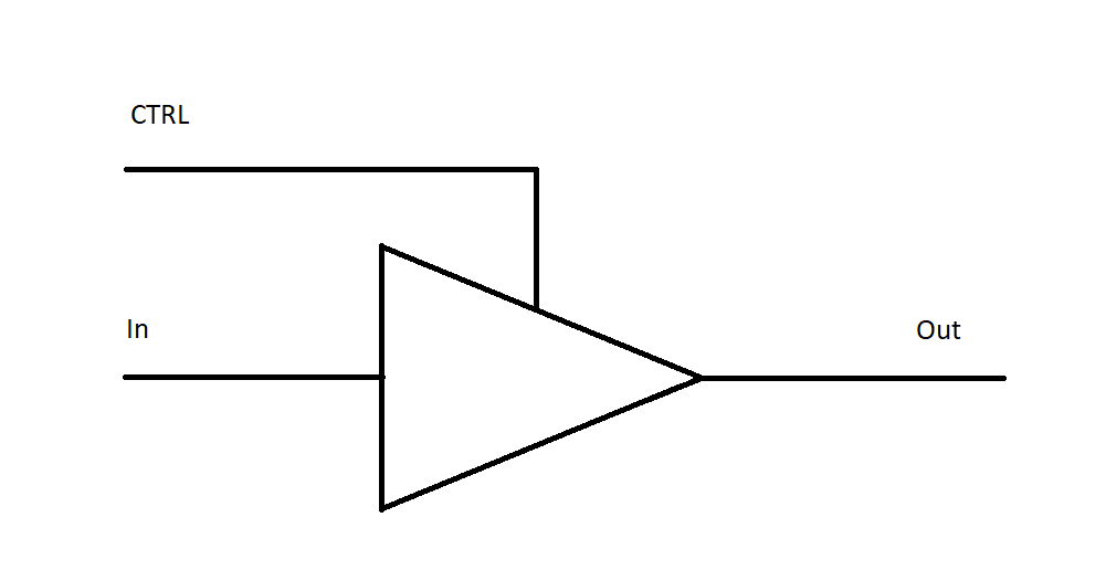
| CTRL | In | Out | |
|---|---|---|---|
| 0 | 0 | Z | |
| 0 | 1 | Z | |
| 1 | 0 | 0 | |
| 1 | 1 | 1 |
The device has two inputs - one for data (In) and one for controlling the state of the output (CTRL). When CTRL is 1, the input is passed straight to the output without alteration - basically, a wire.
When CTRL is 0, the output is forced to the Z “High impedance” state, effectively “unplugging” input from output. Basically, a broken wire.
The usefulness of such a device is that it enables us to physically connect multiple digital device outputs to the same physical wire, and select which one of them is electrically connected to the wire. This selection ability means we can control which device dictates the binary 1/0 state of the bus.
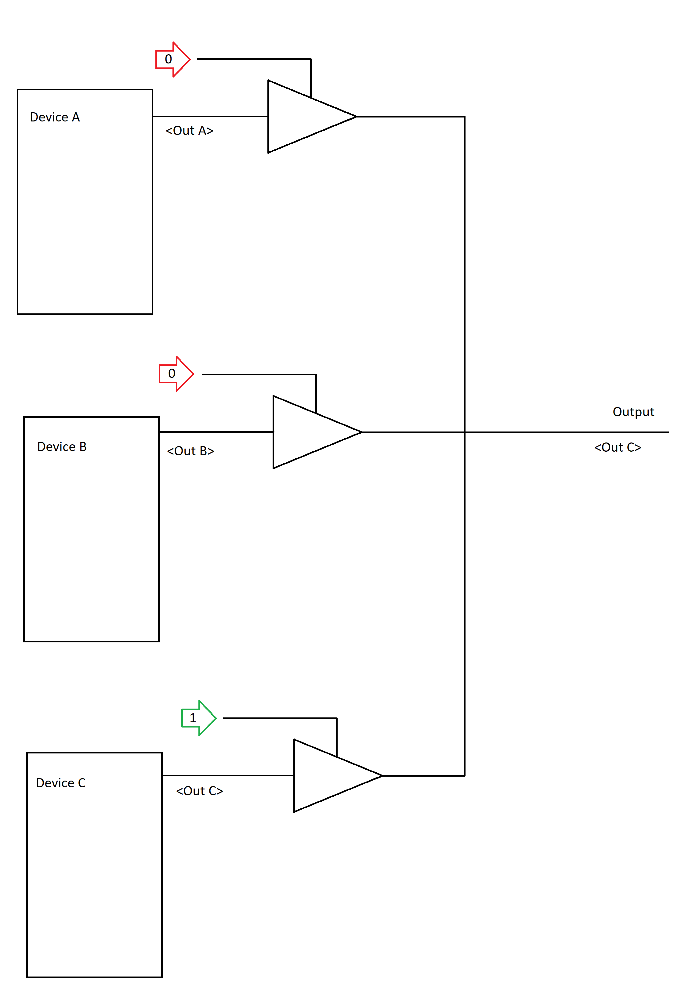
Here we see three digital devices with outputs linked. Since the buffer at the output of C has a control signal of 1, we know the final output will be the same as C. It can be said then that Digital Device C is controlling Output.
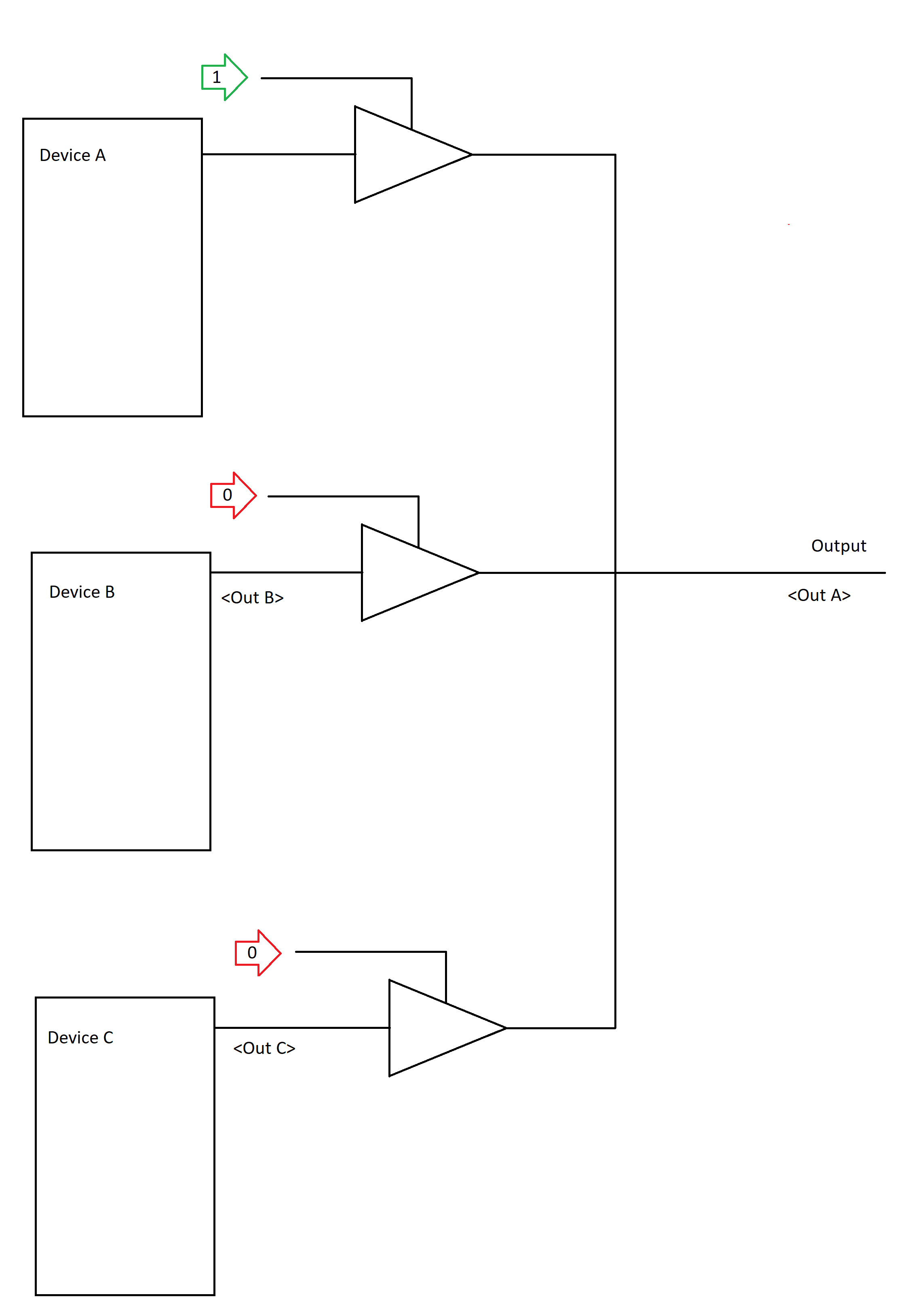
Similarly, we can setup A to control Output by turning off CTRL for C, and then turning on CTRL for A.
When you have a setup like this:
- The wire downstream of all of the tri-state buffers is referred to as the “Bus”.
- When the tri-state buffer is active, the device is said to assert its output onto the bus.
- When the tri-state buffer is active, the device is active on the bus.
Obviously this is a 1-bit demonstration, but you can easily put 8, 32, or 64 of these together to make a bus that is one word wide. The number of bits in a bus is its width.
As readers may have already noticed - only one device can assert its output onto the bus at the same time. If two devices attempt to assert onto the bus at the same time, and they assert different boolean values, you’ll find yourself with a short circuit and magic smoke in no time. For this reason, the devices have to be coordinated somehow to ensure only one is active on the bus at a time.
The System Data Bus
System Data bus is a common set of wires that transfers data from one device to another. A quick taste of what’s to come: at the core of the Von Neumann architecture is a data bus that is used by all components to transfer data back and forth. Each device has a set of tri-state buffers on its output so it can selectively take control of the bus, or allow some other device to assert its data. Additionally, each device has some ability to read the value from the bus, and pull it internally (to do something useful with it, presumably?).
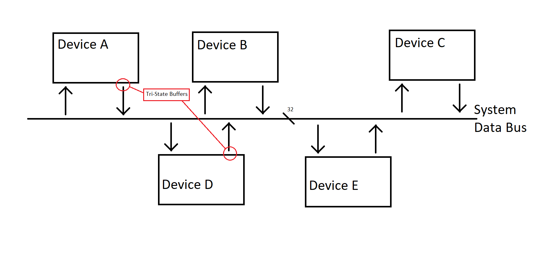
In this case we’ve chosen to draw a 32-bit wide bus (like most processors up till a few years ago had).
Register Load and Store
From previous, we know how to “gang” multiple D flip flops together to make what we call a “register”, which can store one word’s worth of bits.
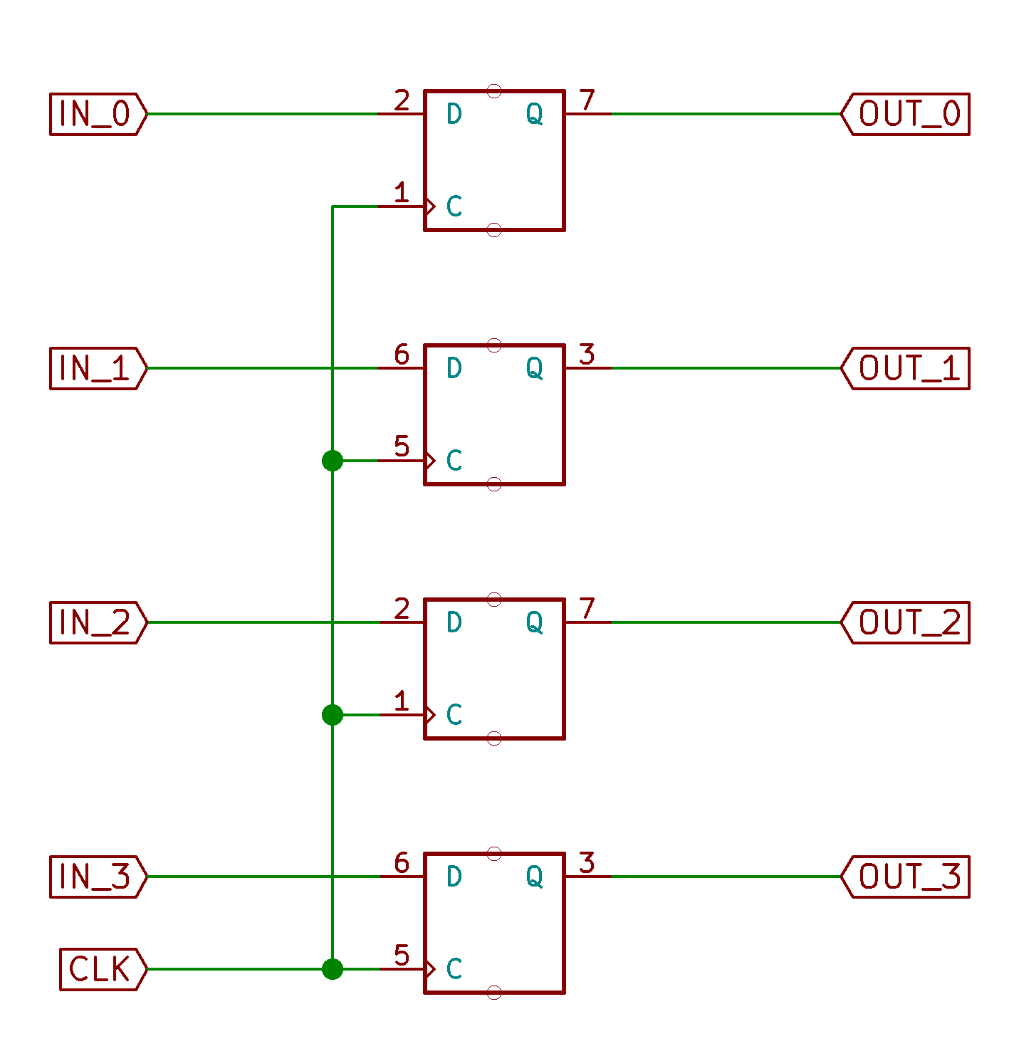
Since we started with a 32-bit bus, let’s also keep 32 bits here.
Along with the system bus, imagine if each device is a slightly modified register. We’ll go ahead and use the little circuit created as part of an alarm clock to put a mux on the input to the register. We’ll also add our tri-state buffer output.
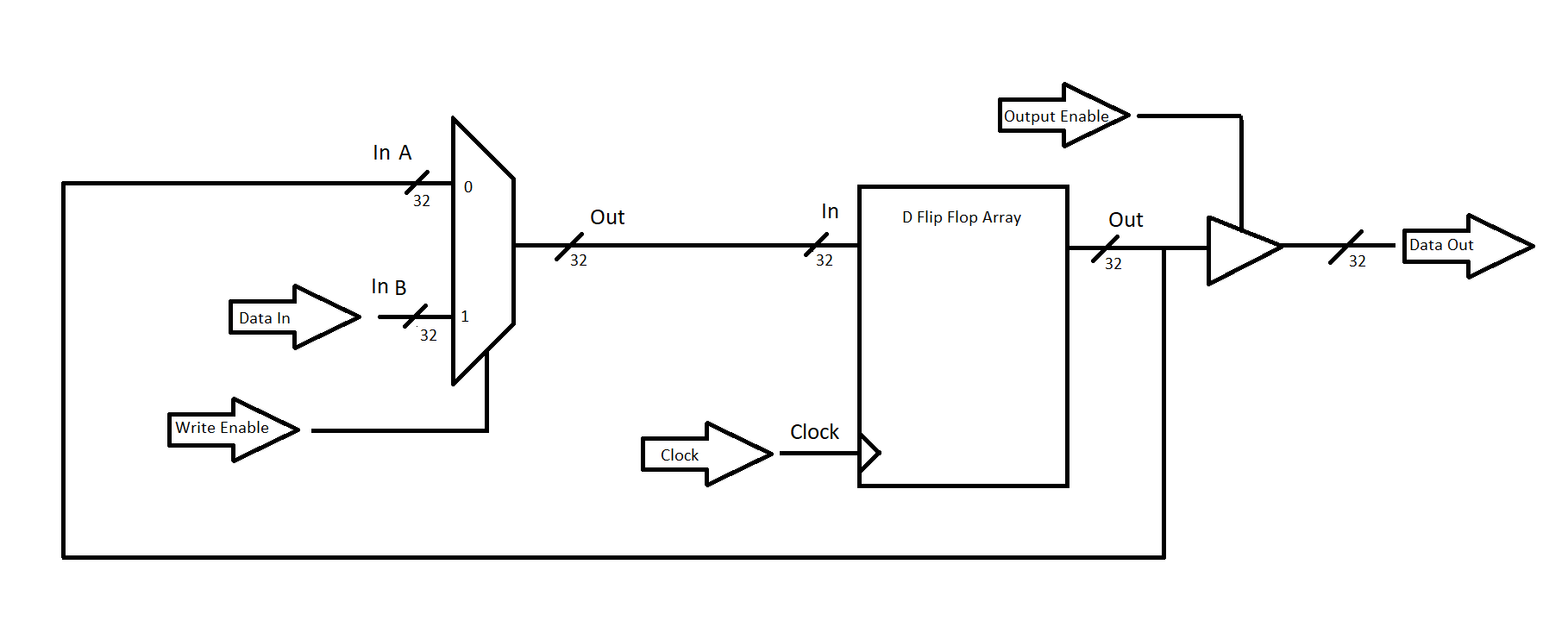
We have the addition of the “Write Enable” enable input to choose whether the register is to load a new value from the data input or preserve its previous value. The “Output Enable” signal allows us to choose whether the output is active or not, allowing this register to be placed as a device on a system data bus with other registers.
We can draw the following symbol for an abstraction of this device:
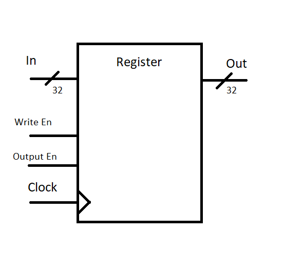
These registers will make up the core of data storage on the processor, and will be a key component going forward.
To demonstrate how they are used, take as an example 3 registers sharing a 32-bit data bus:
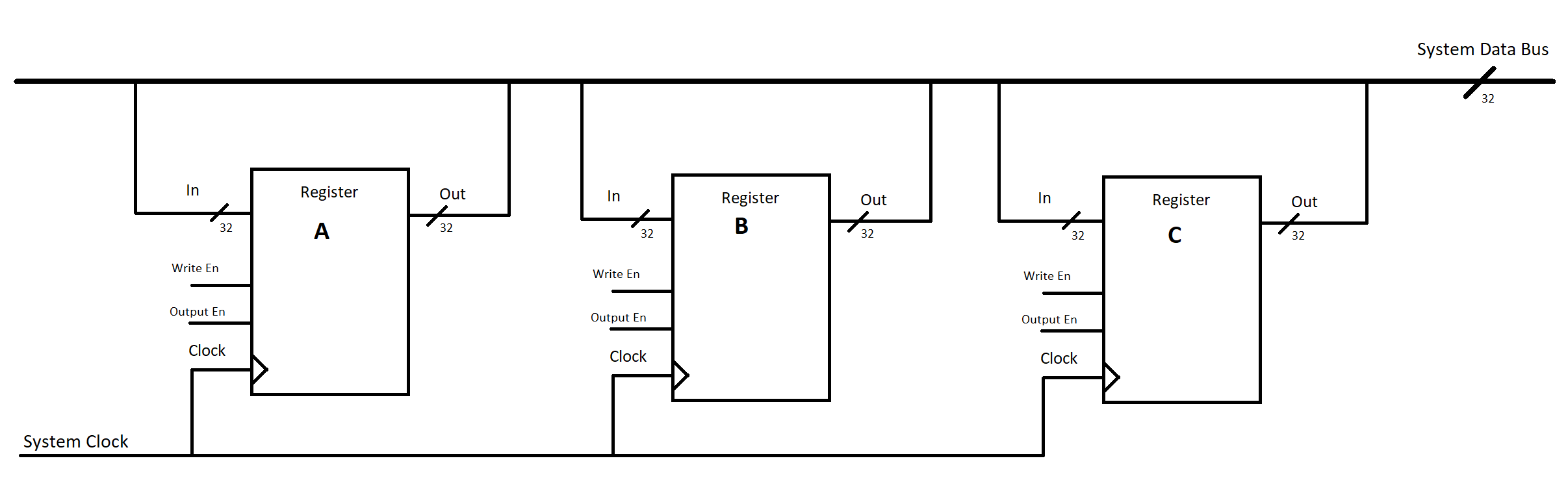
We now have a system where we can systematically transfer data from one register to another. We have to have something coordinating the write & output enables for all of the registers together - however, assuming you do, it’s actually quite easy to move data around now.
Say you have a number in register A that you want to move to register C. Before the clock has a rising edge, you simply set register A’s Output Enable to 1, and register C’s Write Enable to 1 (and everything else to 0). Then, on the rising edge of the clock, the value from A will end up in register C, while B remains unchanged.
We will notate this sort of transfer with a shorthand description:
This simply indicates that on this particular clock cycle, we transfer the value from A into C.
This is often called “Register Transfer Language”, and is the basis of the way we’ll describe how data gets transferred around in a processor. The key to remember is that behind every description of or , it’s just a set of enable bits getting set correctly, such that data flows from from the source to the destination.
Next Steps - Where are we going?
That’s enough history and context-less introduction. Please promptly check out Von Neumann Processor Architecture!
-
For the curious, formal systems of modeling the state of analog electronics in a “digital-useful” way can go up to having 9 states. ↩