People who are more than casually interested in computers should have at least some idea of what the underlying hardware is like. Otherwise the programs they write will be pretty weird. - Donald Knuth
Introduction
Oooh boy, I am getting excited! More excited than a search companion who can do tricks! Things are starting to get very real now!
We’ve introduced a ton of topics in boolean logic - how to manipulate bits, store them, and use them to represent numbers. It’s time to start digging into how all this comes together to build a real device which can do computation!
The Von Neumann Architecture
Overall
Through his work, Von Neumann described a generic architecture for how to construct and lay-out electronic components to fulfill Turing’s requirements. This description has been coined the “Von Neumann Architecture”. It should be noted that since almost all modern processors follow the architecture to some extent, the phrase “Von Neumann Architecture” actually refers more to the set of ideas, rather than one particular design.
Von Neumann divided his world up into four very-high-level components:
- Memory - A device capable of saving and recalling pieces of information.
- Might be broken into multiple parts
- Read-only vs. Read/Write
- Roughly analogous to the “Tape” in the Turing Machine
- Might be broken into multiple parts
- Processor Unit - A device capable of performing a calculation on pieces of information.
- Possible calculations:
- Math (add subtract multiply divide etc.)
- Logic (and or not)
- Comparison (greater than, less than, equal to)
- Roughly equivalent to the “Head” in the Turing Machine
- Possible calculations:
- Control Unit - A device to provide coordination between all other units
- Produces the control signals that configure all other units
- Produces the correct signals to implement the Universal Turing Machine
- IO - A set of devices capable of transforming information between representations useful to computers, and representations useful to humans.
- Screens, mice, keyboards, etc.
- Implementation is device specific, but the key is that on one end is an interface that works well with the computer (bits and bytes), and on the other end is a physical thing a human can manipulate or sense.
- In our Turing Machine association, this is just the way a human can manipulate or interact with the device or the tape.
Processing Unit
Storing data is cool, but to do useful processing we have to, well, process the data. Back when we learned about boolean logic, we saw all sorts of ways to mash bits together. The goal now is to build a circuit which can do all the useful things for us.
The collection of circuitry which does the calculations is generally referred to as the Arithmetic Logic Unit, or ALU. It gets its own fancy-pants symbol that looks like a sideways pair of pants:
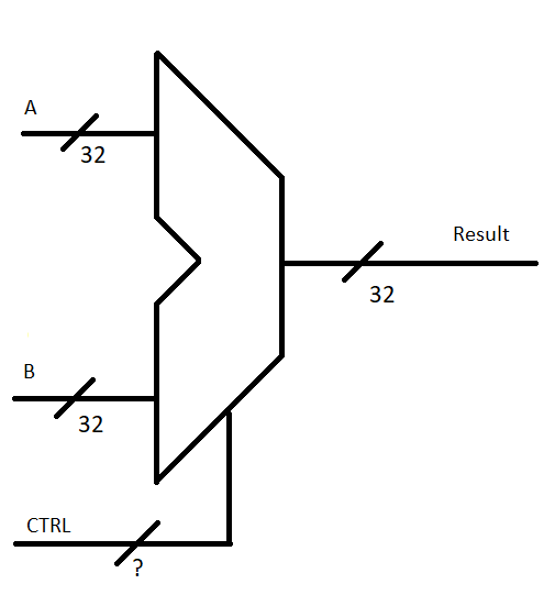
Implementations on various processors will vary slightly, but conceptually they all have to have at least 3 inputs:
- A and B - the operands. A and B are the binary numbers we’re going to mash together
- CTRL - the signals that say how to mash A and B together.
And of course, the set of these three inputs produces the result of the requested calculation.
Keeping with our 32-bit theme, we assume that the ALU is set up to do calculations on 32-bit inputs, and produces a 32-bit result. Other processors may assume otherwise, but this is just our example for now.
CTRL can be any number of bits - it just depends on how many different ways you want to be able to combine the inputs A and B together. For example, if you have 12 combination strategies implemented, you’ll need bits.
The simplest practical architecture I’ve seen has a very small ALU with only three operations supported:
- Bitwise AND
- Bitwise NOT
- Addition
It’s pretty bare-bones. FOr example, to do , , you have to first negate the B operand (which requires a bitwise NOT, then adding 1), then adding A and (-B). Subtraction is a 3 step process, which kinda stinks.
Larger ALU’s will support more operations, including:
- Bitwise OR/NOR/NAND, Subtraction
- Keeps common operations down to a single step
- Multiplication, Integer Division, Remainder after division
- Expanded math abilities on integers
- Note that floating point (decimal) numbers are frequently handled by a different unit
- Bitwise XOR
- Super useful for cryptographic and computer security operations
- Shift bits left and right by one
- super fast way to multiply or divide by 2
- Increment, decrement
- Super-optimized versions of common math operations
What set of operations are supported really just depends on processor design. Increasing the number of supported operations increases speed to a point, but always at increased cost and increased potential for things to break.
Conceptually, putting together an ALU is remarkably straightforward. Just package all the circuits which do the operations you want individually, feed them each off of the provided inputs, and use a MUX driven by the CTRL input to select which calculation makes it to the output.
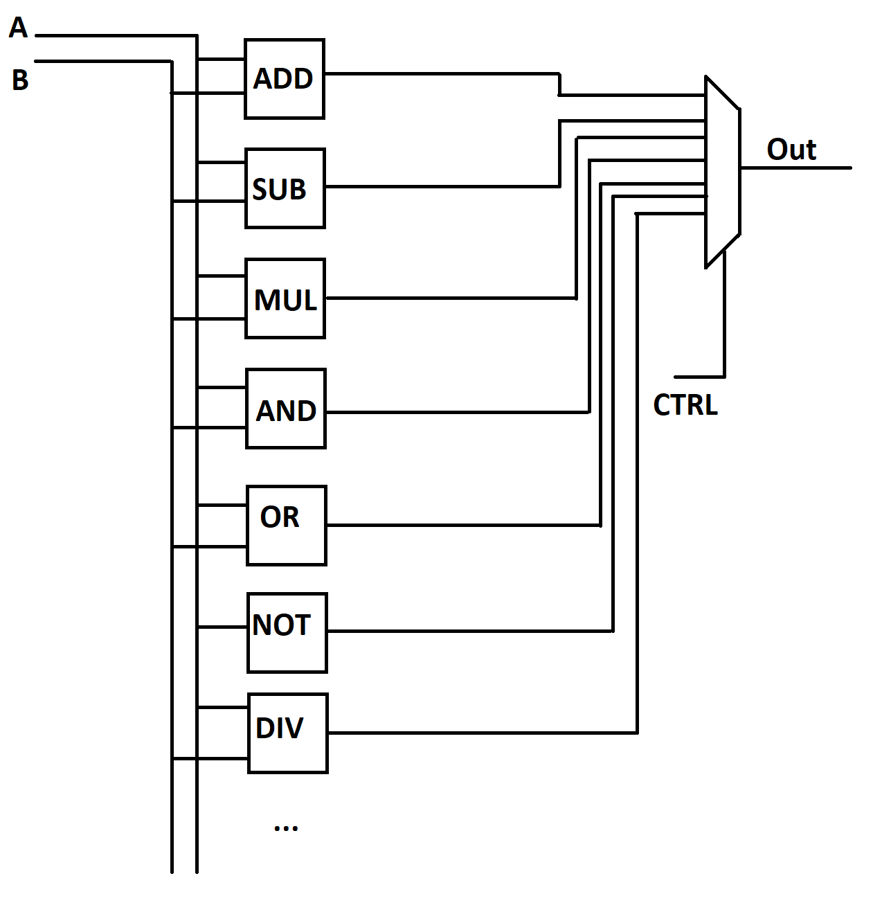
In addition to these combination operations, the ALU will often have additional outputs to indicate if the operation resulted in overflow or underflow (ie, result was outside the min or max range of the numbers that can be represented by the 32 bits of the ALU).
Control Unit
The control unit is the heart of this whole system, coordinating the action of registers and the ALU together to do actual calculation. The design of the unit is special tailored to implement the stored-program concept. Again, the exact design of the control unit can vary, but all have to have at least a few basic components and abilities.
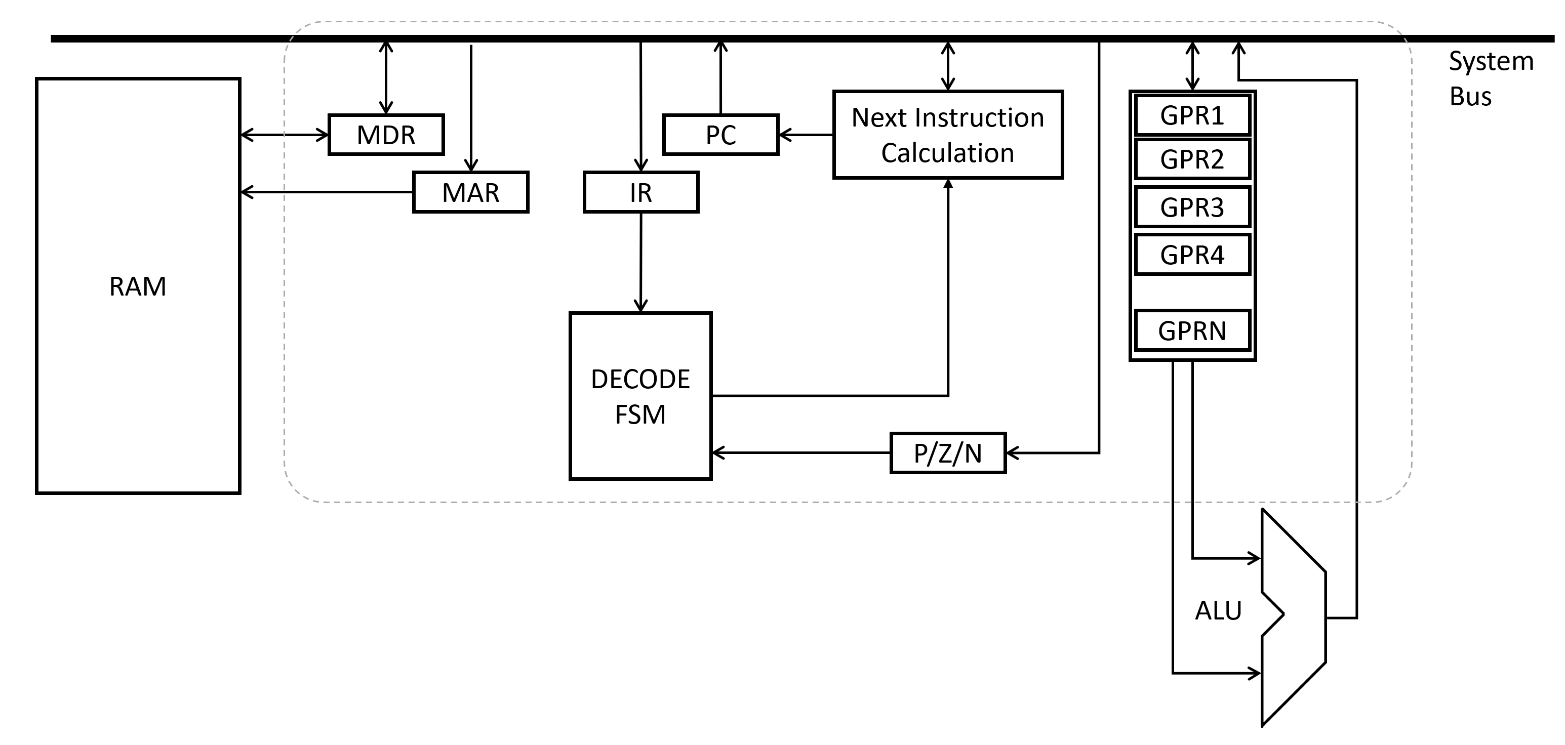
Registers
Fundamentally, every control unit will have a set of registers to store information. These will be faster than the bulk RAM chips you’re familiar with, and serve special uses within the processor. But, fundamentally, they just store a specific set of bits representing some specific, meaningful quantity.
The Memory Address Register (MAR) and Memory Data Register (MDR) are two of the key registers. They are connected directly to the RAM circuitry, and allow the control unit to command unit to read or write from a specific memory address. Along with a couple control signals, the basic process is that the memory address register is first loaded with the desired address. Then, control signals are sent to memory to read or write that address. For read, the data is pulled off the RAM chip and placed into the MDR. Write does similarly, but propagates whatever value was in the MDR (from the control unit’s other parts) and puts it into the address in RAM specified by the MAR. Using this, the control unit can read and write RAM data.
Two more registers form the core of the stored program concept. The processor fundamentally assumes that the instructions it is supposed to execute exist in memory at a certain set of memory instructions. The Program Counter (PC) register stores the memory address of the current instruction being worked on. The Instruction Register (IR) holds the actual instruction while its being worked on.
There are also a set of registers called General Purpose Registers (GPR*). These don’t have a very specific purpose, they are left open for the programmer to use as they see fit while writing programs.
Depending on how the IO devices are designed, there may be some dedicated registers attached to physical, user-interaction input or output devices.
System Bus
As introduced with the tri-state buffer, we know that we can connect multiple digital outputs “together” forming a Bus topology. Von Neumann introduced the idea of a System Bus, where registers (and other components) read and wrote data to a central set of wires. This made interconnects easier, and made checking system functionality more straightforward. Modern processors may use more than one system bus to allow for faster data transfer, but for our purposes we will only consider one.
The Execution Cycle
Most control units follow a repeating three-step process while running:
- Fetch
- Decode
- Execute.
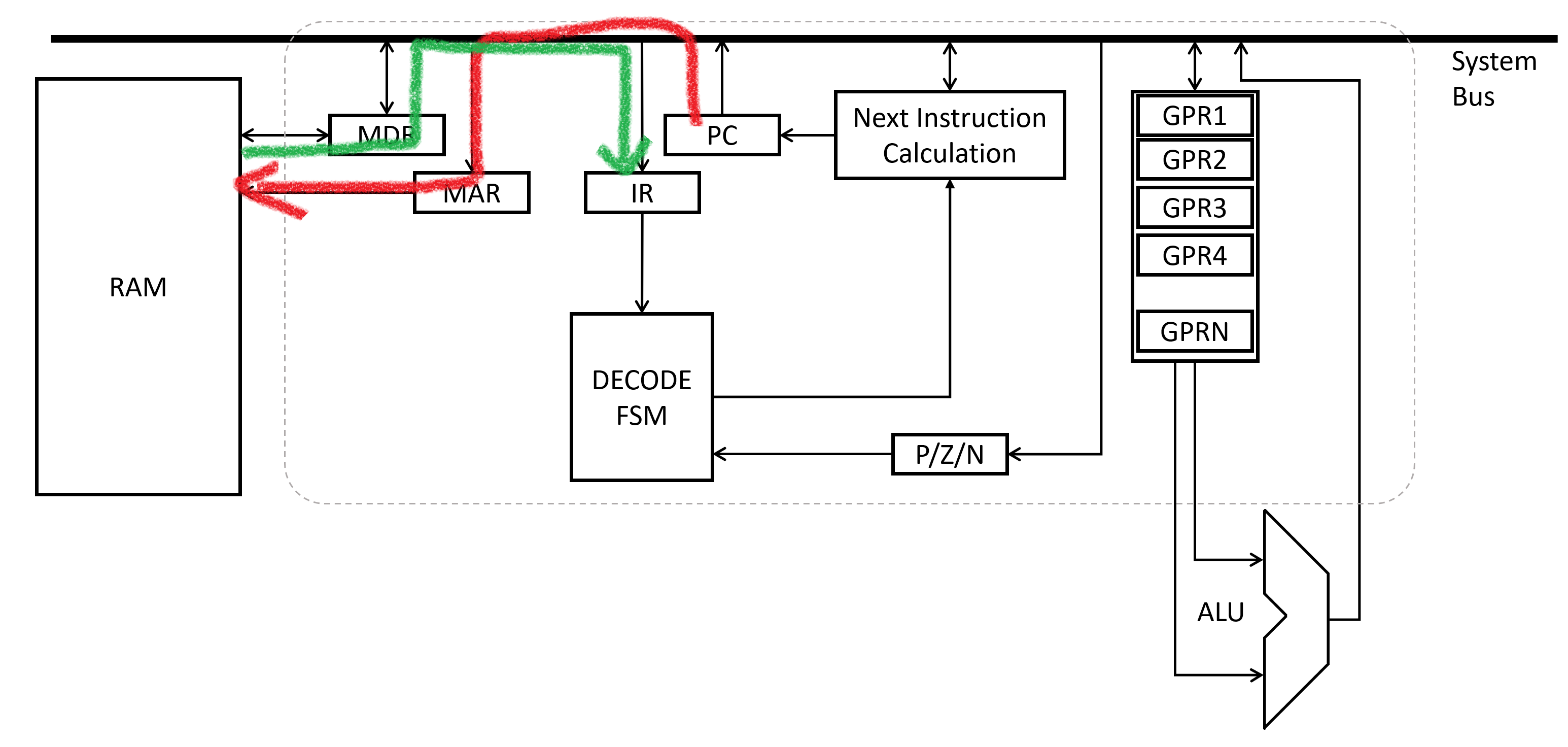
During the Fetch phase, the control unit fetches the next instruction. The Program Counter register is used to populate the Memory Address Register. Then a read is commanded from the RAM chip, and the result in the Memory Data Register is moved to the Instruction Register.
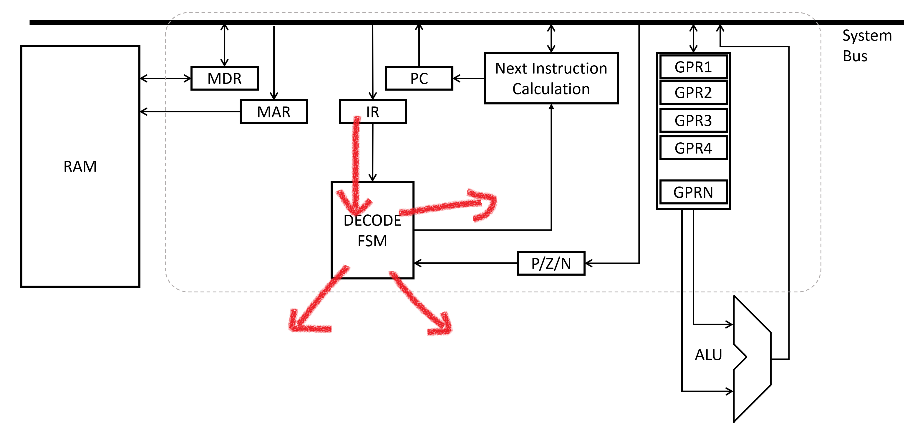
During the Decode phase, the contents of the instruction are analyzed to see what is commanded. Control signals to other parts of the processor are adjusted based on the contents of the instruction.
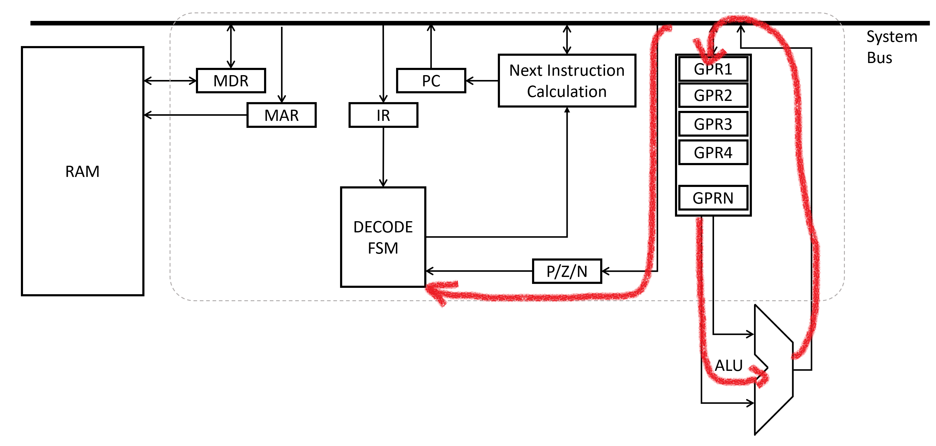
During the Execute phase, the actual requested actions are carried out. The Program Counter is updated to a new value (usually the next memory address in sequence). The drawing above shows an example where the ALU is used to do math.
Decoding & Executing an Instruction
Generally, instructions will command manipulations to registers. Some examples of these:
- Math - Add two general purpose registers, and store the result in a 3rd general purpose register
- Memory - Load a general purpose register from RAM, or store its contents to RAM
- “Branching” - Manually adjust the Program Counter if the previous instruction’s result was positive
- IO - reading/writing from some input or output device.
Instructions will always have two main components: the opcode and the arguments.
Remember that each instruction is just a set of bits. Usually, the first couple bits is the opcode, which identify what the instruction is requesting.
The exact mapping of which bits equate to which operations is dependant on the details of the processor construction. Here’s an example from x86, which is by far one of the more complex versions.
Simpler machines might have a mapping more like:
| opcode | Abrev. | Meaning | |
|---|---|---|---|
| 0001 | Add | Add two numbers | |
| 0010 | Sub | Subtract two numbers | |
| 0011 | OR | Bitwise OR of two numbers | |
| 0100 | AND | Bitwise AND of two numbers | |
| 0101 | NOT | Bitwise NOT of a numbers | |
| 0111 | STR | Store a value to memory | |
| 1000 | LD | Load a value from memory | |
| 1001 | BRN | Branch to a different instruction if the previous result was negative | |
| 1010 | BRZ | Branch to a different instruction if the previous result was zero |
And so on. Note that when you see assembly instructions, you’ll almost always see it referred to by its abbreviation, not by the 1’s and 0’s of the opcode. It’s hard to stare at the 1’s a 0’s, your eyes start to go crossed after a while.
The remaining bits are dedicated to the arguments to the opcode. They indicate the specifics of how the processor is to carry out the instruction.
For instructions like Add, Subtract, AND, OR, etc. - the simplest set of arguments indicates a trio of general purpose registers to work with. Usually the arguments will be specified to say “source 1 register”, “source 2 register”, and “result register”. NOT would only need two registers, but is conceptually the same. When the Instruction Register has AND for an opcode, the control unit will use the arguments to configure the signal routing in the processor to pipe the two source register outputs into the ALU, and then the ALU’s output into the result register. One tick of the system clock goes by, the result register is updated, and the instruction is completed!
Opcodes that work with memory addresses (BRN/BRZ,LD/STR) will often make one of the arguments the memory address to work with. More complex “addressing modes” allow the address to be specified relative to the program counter, or some general purpose register.
Choosing the Next Instruction
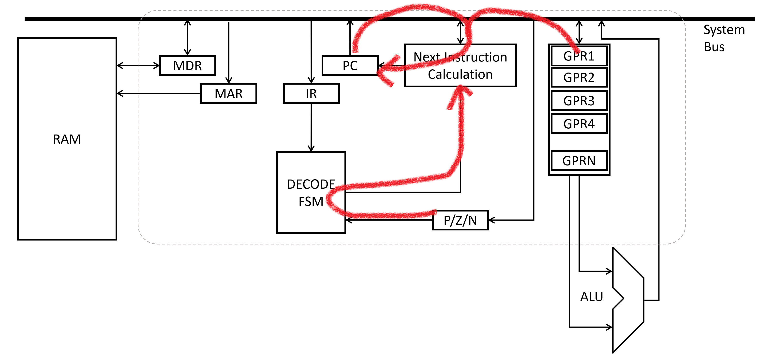
Generally, after all decoding and execution has been completed, the Program Counter has to be updated with the next address. Frequently, this just means “add one” to the current program counter. However, the instruction might have some more complex instruction. “Branch” instructions generally alter the add-one behavior conditionally, based on the previous result being positive, zero, or negative (PZN register stores this information every instruction cycle).
The manner in which they alter it can vary far and wide. Usually it involves some offset from the current PC - rather than going to the next instruction, you skip forward by some larger number of addresses, or maybe backward by five addresses… something like that. The size of the jump may be encoded into the instruction word itself, or pulled from a general purpose register, or lots of other options really. At the end of the day, it’s just up to how the instruction is interpreted again to select which calculation is used to update the PC prior to the next execution cycle.
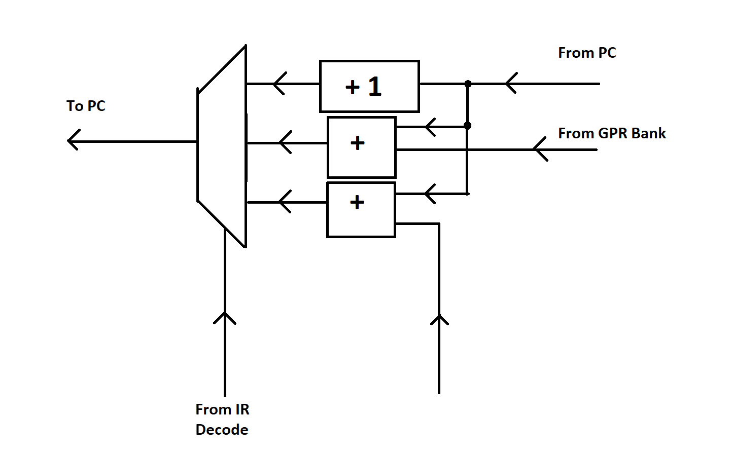
The net result is the same though - the PC gets loaded with the address of the next instruction to run, and the cycle may start over!
IO techniques
In general, any input and output device will have to interact with the processor via some set of bits. For example, a mouse might report its X/Y coordinates as two integers. A screen might require representing every pixel color with one byte of data. Regardless of how it’s actually done, just keep in mind that at the end of the day, it’s just a set of bits that are read from, or go to, the device.
How the processor gets access to these bits happens through two primary methods:
Port Mapped
Some processors will have dedicated registers inside the control unit for reading and writing data associated with a user IO device. This also means there will have to be dedicated assembly instructions for manipulating that data as part of a program. THis is a very fast method, but can be a bit inflexible, as the processor has to be designed with assumptions about what its IO devices will be. This is bad if you plug or unplug a device from your computer.
Memory Mapped
Sometimes, a more flexible technique is to use the same interface the RAM circuitry uses. The IO device “poses” as part of the RAM chip, responding to processor read and write requests just as a RAM chip would. But, rather than storing and recalling data as requested by a processor, the “other end” of each byte is hooked up to some IO device.
This means there are no special assembly instructions required to do IO interaction. As a software writer, you just have to know things like “Memory addresses 0x0000154A and 0x0000154B are mouse X/Y” and “Memory addresses 0x00002000 through 0x00002FFF control the pixels on the screen”. Don’t use these special memory addresses like normal memory (ie, writing to the mouse addresses will probably not end well). But, it’s much more flexible than forcing a Port Mapped architecture.
But, there are plenty of tradeoffs on both sides. You’ll probably see both as you adventure into this wonderful world of processors!
Concrete Examples of Architecture
So far, we’ve stuck to generic descriptions of the common things you find inside a processor. Lots of descriptions have just been these hand-wavey “well the actual implementation depends on the processor type”. For the curious, we now present three concrete examples of computer architecure.
LC-3
The “LC-3”, or “Little Computer 3”, is a “fake” architecture. You’ll not find an off-the-shelf chip that implements the “LC-3” architecture. But, it’s a dirt simple architecture - fixed opcode and word widths, simple operations, conveniently sized RAM… the list goes on.
There are a good number of online resources that explain the architecture - some even down to the gate level. It’s simple enough that the blog author implemented the processor, gate level up, as part of a sophomore year elective class.1
It’s a great place to start, but unfortunately doesn’t directly map to any real architecture. However, the concepts you learn while studying it definitely do apply!
x86
x86 Processor Architecture comes from Intel, and dates back to the late 1970’s. Over the years they have added lots and lots of new instructions to it, expanded the data width size, and a whole slew of other alterations, all while keeping the base thing backward compatible. This makes for a very versatile and very powerful processor. The biggest downsides are all rooted in the complexity of the devices - infinite backward compatibility makes for a lot of “legacy” portions of the architecture that aren’t relevant for modern programming. Additionally, you need a lot of gates to make an x86 processor, which generally means they are power hungry (though this has been mitigated in recent years).
Still, the sheer flexibility and power of the architecture means almost every desktop PC (running Windows, Mac, or Linux) has some form of an x86 processor in it, and tons of manufacturers produce a flavor of the architecture.
This was the second assembly language the author learned. Along with three other students, he wrote an operating system from scratch using C and x86 assembly. 2
ARM
Advanced RISC Machine architecture is the new “big kid” on the block. Specifically designed to address some of the x86 shortcomings, it quickly made a name for itself for its simplicity of implementation (therefor requiring fewer transistors, and drawing less power). It came along at just the right time to be adopted by the smartphone revolution, and nearly all smartphones on the market today run some form of this processor. It’s strongly suited toward running mobile, power-sensitive applications. The roboRIO uses an ARM Cortex-A9 processor manufactured by Xilinx.
The Place of the Special-Purpose Computing Device
This whole blog post, we’ve been discussing how to made a digital device which can perform general purpose computation. This isn’t to say that general purpose computers are the be-all, end-all of computation. Indeed, the ability to be programmed brings overhead with it. In the fetch/decode/execute cycle, fetch and decode are both only present because the processor has to figure out what it is supposed to be doing at runtime, in addition to actually doing it.
For this reason, when bleeding edge speed or absolutely minimal power consumption is required, it sometimes still makes sense to give up the ability to be programmed to gain that speed or efficiency. Digital Devices can still be custom designed to fit a very specific purpose. These are often called Application Specific Integrated Circuits (ASIC’s).
Common applications include video/audio processing, computer networking devices, and scientific research equipment.
Conclusion
Phew, that was a lot, and way more hand-wavey than I had initially intended. None the less, we still have built up an understanding of what the main components of a processor are, how those things come to be from smaller digital circuits, and how they can execute individual stored instructions.
Next up, we’ll take a survey of common programming language constructs, and later dig into how those constructs might be implemented in assembly code. Keep reading at Programming Languages Introduction!.
-
Lots of students post their solutions on github, which seems like a violation of academic integrity, if you ask me. ↩
-
Again, lots of students decided to post their solutions online. Tisk tisk. ↩