This post is the continuation of Part 1 in our series on digital devices.
Combinational versus Sequential Logic
So far, we have discussed circuits which take a set of inputs, and produce an output. They do not “remember” any particular piece of information - their outputs are a function current inputs only. They keep no record of past inputs. These are called Combinational Logic circuits.
As we mentioned earlier in the case of the astronaut button, sometimes it is useful to remember information about past information. Circuitry which accomplishes this memory is called Sequential Logic.
All the logic gates we’ve shown so far are by themselves combinational devices. However, we’ll now introduce a class of devices where outputs are carefully fed back into inputs, allowing the device to retain information over time. We will be able to build these up into a full RAM chip, just like you have on your computer to store information!
Flip Flop
The most fundamental unit of memory storage is usually referred to as a flip flop. Much like the beach-oriented footwear, they flip and flop back and forth between true and false, with transitions triggered by certain input conditions. They also come in a number of different flavors. The easiest to analyze at first is often called the “SR Latch”, which we’ll look into as an example. Then we’ll abstract away the details and talk about a few other varieties.
Gate Propagation Delay
One thing we haven’t touched on yet - how long does it take a gate to do a calculation? So far we’ve kinda just ignored it - effectively assumed the answer is “infinitely fast”. Of course, nothing is infinitely fast. Voltages can’t change instantaneously, electrons take time to move around! When you apply a certain input combination to a gate, the reaction is quite quick - usually on the order of nanoseconds. However, it’s not literally instantaneous. Propagation delay is the name given to this duration between applying inputs, and seeing the correct output.
This is yet another example of abstraction. For combinational logic, we are able to ignore this gate delay - assuming it is faster than anything we would ever care about (ie instantaneous). For sequential logic, understanding the function of our new flip-flop friends requires we at least keep this delay in mind.
Basic Flip Flop Ideas
The key to any flip-flop - we take the output, and route it back to an input. Due to gate delay, this effectively makes the “previous output” an input. When the previous output is an input, we can use it to remember what the output used to be. With some clever design, we can in fact make some useful memory happen.
The SR Latch consists of two cross-coupled NAND gates, hooked up like this:
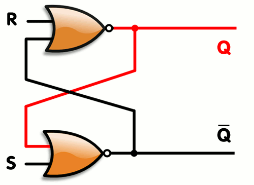
Wikipedia has the best picture of this I’ve seen so far, so I use theirs.
The input is for “Set”, and the input is for “Reset”. The output is named . Note by the GIF:
- When you set to 1 and to 0, this will cause the output to go to 1
- When you set to 0 and to 1, this will cause the output to go to 0
- When you set both and to 0, it causes to maintain its value
Number 3 is the magic of the device - by leaving both inputs at 0, your output retains its previous value. This illustrates how you can hook gates up in a way to remember something about the previous inputs.
Note how the loop-back of outputs back into input only makes sense if you assume gate delays are present. There is a very slight delay between a change in input and a change in output, as shown in the gif. If you assume things change instantaneously, you get logical conflicts and are setting 1 equal to 0 (which implies a short circuit, which usually means magic smoke is getting out ). But, due to gate delays, for carefully designed circuits this is not a problem. When you buy the real chips that have SR Latches in them, the silicon has been carefully designed to make the gate delays just right so this all works out. And then you as the user don’t have to worry about it. Yay abstraction!
The astute reader may notice that there is a key flaw 1 to this configuration: Look what happens if you set both inputs to 1. Starting near - , meaning is equal to . Wait a minute. True can’t be equal to False. Huh.
In reality what happens here depends on how your gates are constructed with transistors (you have to go one layer down in the layers of abstraction). You might get oscillation, or maybe short circuits and magic smoke. Depends. No matter what, setting both inputs to 1 is a bad idea. Due to this, it’s common to put additional gates in front of the S and R inputs to facilitate ensuring you never get the latch into a wacky state.
The Clock Signal
To properly motivate the specific flavor of flip-flop that we will be talking about, we will first take a tangent into a bit of processor design.
Think about when you read about specifications for a processor. One of the most common specs you read about is the processor’s speed, which is measured in some units of Hertz. Modern desktop processors are rated to run at around 2 to 3 GHz (Giga-Hertz, or Cycles per Second). This speed rating roughly corresponds to the number of operations the processor can do per second. But what it really references to is the clock speed of the processor 2.
The clock in a digital circuit is just a specially-designated signal. The clock cycles repeatedly between 1 and 0 and 1 and 0 at some specific frequency. Digital devices are designed to take a clock signal as one of their inputs to help it to stay in synchronization with other devices in the system.
Circuits are designed such that at every edge of the clock, or every transition from 0 to 1 (or so we will assume for now), it is assumed that all inputs to a particular digital device are stable and therefore available
The maximum clock speed is dictated by the worst-case propagation delay from the circuits that make up the system. If you have constructed some circuit with 10 AND gates passing each output to the next one’s input - you have to wait 10 times the gate delay before you know that your output is stable. Assuming that output goes to another circuit’s input, and they share a clock, you can’t run your clock faster than each portion of the circuit can update the inputs of the next portion.
This is why reducing the number of layers of gates is important - the fewer layers you have, the less input to output delay you have, and the faster you can run your digital circuit’s clock. This means faster computation, which is generally regarded as a good thing!3.
But Mommy, Where do Baby Clocks Come From?
Don’t worry child, we will tell you when you are older.
Actually, it doesn’t matter too much for our design purposes. This is the beauty of abstraction - you don’t need to know how a clock signal is generated to use it. But for the curious, we will indulge you momentarily.
A clock is just a repeating waveform, and can be derived from any repeating pattern in nature. Common ways of generating it include:
- Getting it from the power line (usually a nice 60Hz in North America, unless your power company screws up.)
- Repeatedly charging and discharging a capacitor through a resistor and a non-linear switching circuit (for example, see “555 timer” circuit design).
- Amplifying the vibrations of a specially-designed crystal made of quartz.
- Using lasers to toss caesium atoms in the air then measuring their atomic energy state decay.
- A whole host of other things
In addition, there’s a whole science to distributing this clock signal carefully to all the circuit elements, so they actually receive nice clean 0-to-1 transitions at the same time. Especially when clock frequencies get high, those wires inside your processor start to act less like ideal wires, and more like radio antennas. It gets mucky fast.
We don’t like to think about all this at once. So we use our powers of abstraction to simply say we trust a clock signal exists and works well, now we will use it.
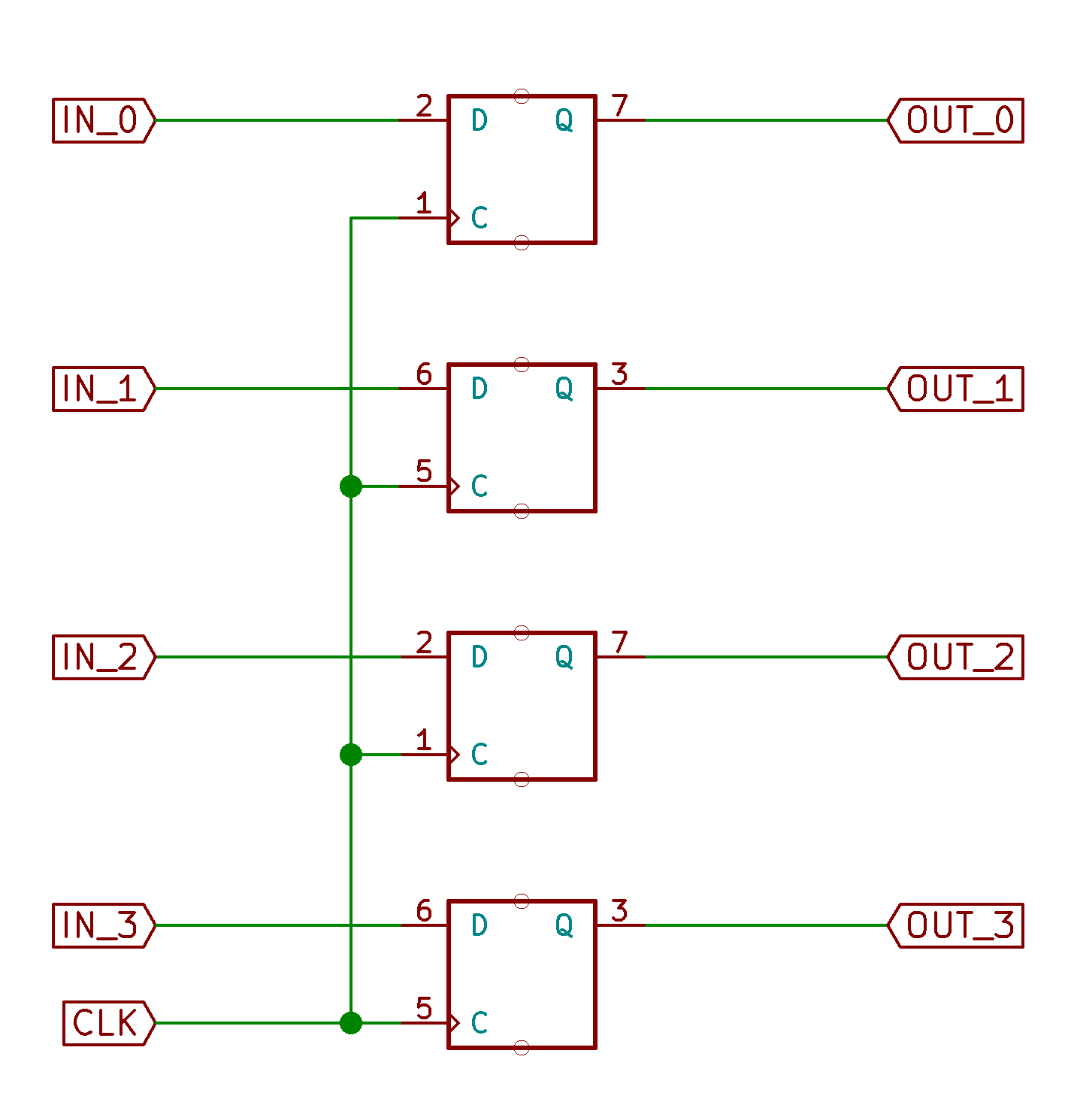
The D flip-flop from Gates.
Here’s our design goal - we want to build a device where we can predictably control when the output changes based on some clock signal input. We will have a single input that dictates when the next output will be, and when the clock input changes from 0 to 1, we will update our output to match our input. At all other times, the output should retain its state.
We do this by cascading multiple SR latches together, such that an input, or some feedback value, “drops through” each layer as the clock swings from 0 to 1. Neglecting gate propagation delay, the 0 to 1 rising edge of the clock will be the event that ultimately causes a new input to appear at the output.
I am again in debt to Wikipedia for providing some images of gate configurations. Far easier than drawing it myself, and equally correct.

It might be a bit hard to trace the functionality, but it’s actually pretty straightforward. When the input labeled Clock goes from a 0 to a 1, the output takes on whatever value is applied at the input. is of course always the inverse of .
Abstraction
When you draw out one of these devices in a circuit diagram, it’s actually confusing to do it with gates. Astute document readers might recognize “oh that’s a D flip flop!”. But in reality, you don’t want to make people think about that, you just want them to know it. So, there’s a fairly generic symbol that gets drawn:

The ports are labeled about as you’d expect from above. The little notched indicates the clock input.
The and ports are often omitted from other drawings. They will force the output to 1 () or 0 () immediately, regardless of the value of the clock or . This is useful for a reset circuit, which (when activated) puts all the devices into a known state. This is useful when first powering on (or rebooting) your computer - depending on the exact transistor layout, the state of each flip flop may not be guaranteed when you first apply power to the circuit. Some might be 1, some might be 0…who knows. To get around this, designers usually just build in the ability to force every piece of the circuit to a known state.
But, Why a Clock?
The reason for triggering on the rising edge is for synchronization across the larger system. Think about a computer chip - you’ll have many many many of these memory components spread throughout your processor, RAM, peripherals, device drivers, etc. You want to be sure that they all change state at the same time, so you design your circuit with a rising-edge paradigm in mind. Namely - when the clock is not having a rising edge, you have that whole time to do all the combinational logic. Signals propagate around, change gate state, do calculations and whatnot…. you can do whatever you like in this time, just as long as all Flip Flop inputs and stable before the next clock rising edge.
For the sake of completeness, it should be noted that digital circuits are often falling edge triggered. This changes the circuit design a bit, but the concept remains the same. It doesn’t matter if your clock goes “1 0 1 0…” or “0 1 0 1…”. General design principles would say to keep all your devices the same - all rising edge or all falling edge triggered. But even this can be violated if you’re careful enough. Not worth focusing on too much now, but just for awareness - rising-ege isn’t the only option.
Counter
Let’s put together a circuit combining two things we have just learned about - adders and flip flops. Our goal will be to build a device which keeps track of time, counting the number of clock cycles. To keep things simple, we’re going to pretend that we’re building a clock for planet Zorgon. It’s a zippy but precise planet, revolving once around its axis once every 16 seconds exactly. Our Zorgon clock therefor just needs to count up from 0 to 15 to track all the seconds in the day, then reset back to 0 after the 15th second (when it is the next day).
If you recall from the binary lesson, if we have 4 bits and treat them as an unsigned integer, we can exactly represent the numbers 0 through 15 (since )). They don’t call Zorgon the “Planet of Simplifying Mathematical Coincidences” for nothing!
To store the present time, we will use 4 D flip flops in parallel. This is nothing fancy, just creating a new digital device with three main ports. A 4-bit input, with one bit going to the input each flip flop. The 4-bit output comes directly from the individual bits at the output of each flip flop. The clock input is still one bit, and drives all flip flop clocks simultaneously. Effectively, we’ve created a flip flop that stores 4 bits at a time, rather than one. This device is often called a register4.
Rather than drawing all 4 gates every time, we’ll put all this in a nice little box labeled “Register”:
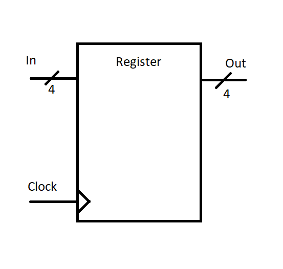
Note the little “/” marks on the input and output ports with the number below it. That’s just a notation way to say “here are four wires that should remain together”. You should always think of those four bits together as representing “time of day”, so we’ll draw them together to help not confuse the reader. Some programs may use a thicker line to show the “bundle” of data wires.
We will make the assumption that we have a clock signal that already runs at 1 Hz (this is not hard to create). Hz (abbreviation for “Hertz”) means “cycles per second”. Since each cycle of the clock waveform has exactly one rising edge and one falling edge, we expect once per second our (rising edge triggered) flip flops will propagate their input to the output.
Here’s the key to the design: the output of the register will be used to represent the present time on Zorgon. Every rising edge of the clock, we will want to increase the present time by 1 (since, of course, time goes forward). To do this, we need to ensure that at all times, the input to the register is the current time, plus 1. This will ensure that when the clock has a rising edge, the new time (cur_time + 1) is propagated to the output, and the output (representing current time) updates properly.
We’ll take a quick shortcut to represent our four bit adder from last time as one block:
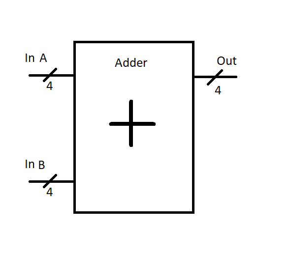
“Inside the box” we’ve accounted for the fact that the carry-in signal is hardcoded to 0, and the carry out signal is unused and not connected.
We’ll hook up a circuit like this:
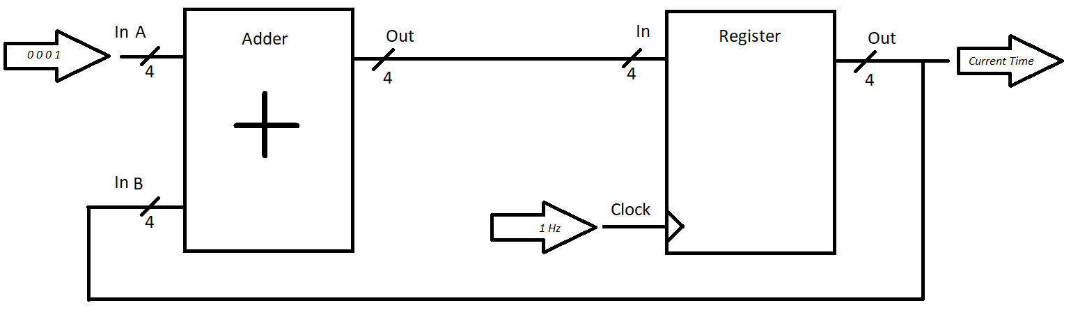
We see our 4-bit ripple carry adder, like we had last time. That “constant value” of 1 is achieved by simply connecting the 0th bit to a high voltage, and all the other bits to ground.
There! With just a few components, we’re able to create a circuit that keeps track of the present time of (Zorgon) day, and outputs it in a binary format!
A Zorgon Alarm Clock
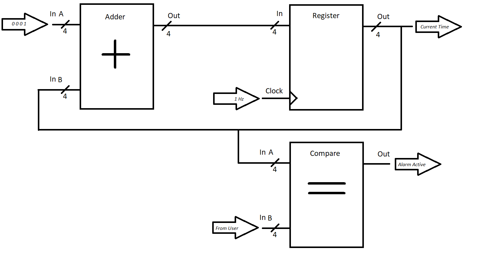
Knowing the current time of day is cool, but what if you want to be notified at a certain time every day? Say, for example, the time you want to wake up at! This is a device most folks would call an alarm clock. As the english name suggests, we could start with our clock, and add an alarm circuit to it.
The alarm circuit is simple. We shall define it as such: it takes two inputs: the current time of day, and the desired time of alarm. Current time comes from our existing clock circuit, and desired alarm time has to come as input from the user. If you want to be woken up by your alarm on the 4th second of the day, you would provide the input bits . Providing user input in digital circuits like this is usually just done through switches that selectively tie digital signals to ground or 5V. Something like this - you’ve possibly seen these in old garage door openers? Maybe? Or maybe I’m getting old.
In any case, we will define that the output of our alarm circuitry is a single bit. It shall be 1 when the current time matches the alarm time, and 0 otherwise. We’ll assume it’s hooked up to some loud buzzer, or a motor that drives a 2x4 into your skull, or releases a flock of penguins, or something “alerting” of that nature. But through the power of abstraction, we will simply leave it at 1 = “alert” and 0 = “no alert”.
To calculate the output, we need to calculate if the two inputs are exactly equal. Doing this across four bits is quite trivial - for two four-bit numbers to be exactly equal, it just means that every one of their bits is equal.
Recall that the output of an XOR gate reports when two bits are different (1 for different, 0 for same). By putting an inverter on the output of an XOR gate, we’ve created an XNOR gate, which produces 1 when the bits are the same, but 0 when they are different.
Similarly, a 4-input AND gate will output 1 when all 4 inputs are true, and 0 otherwise (1 or more inputs are 0).
Combining these together in a circuit like this, we create a simple box which outputs a boolean to indicate “are my two 4-bit inputs exactly equal” 4:
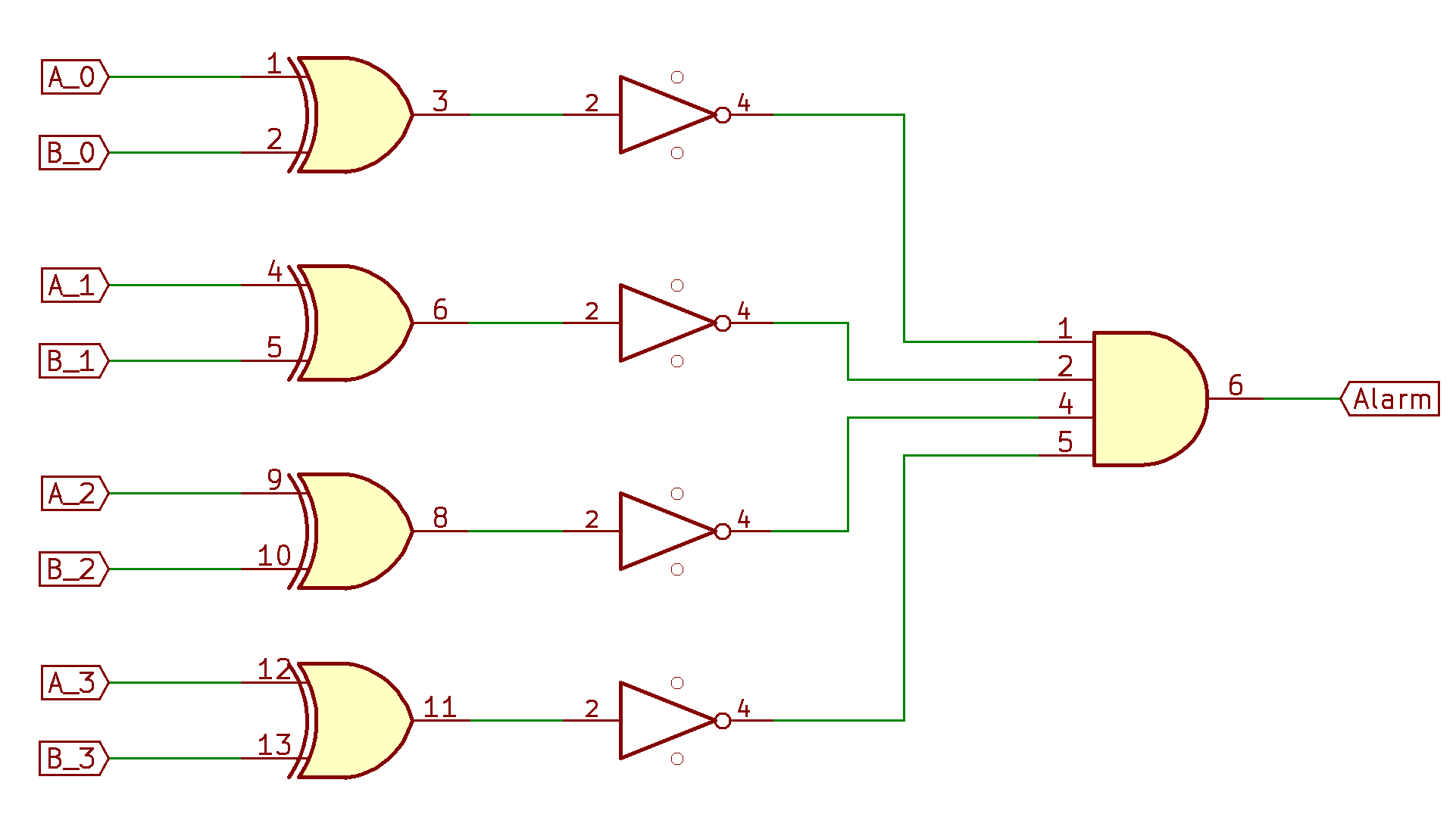
Here we’ve used names A and B for the 4-bit inputs (A consists of A_0, A_1, A_2, and A_3). A is the current time, B is the set time from the user (though order technically won’t matter).
We’ll wrap this circuit up into a nice little box that compares two four-bit numbers for equality:
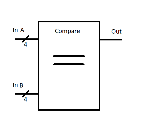
We can then hook this guy up to our existing clock circuit, and we suddenly can be woken up at the proper time on planet Zorgon!
Huzzah!
Too close to home
“But But But!”, you say. “We live on planet Earth! A Zorgon clock is useless for day to day life!”. I hear you, and do not disagree. Let’s think through what we’d have to do to make this clock work on Earth (where there are seconds in one day).
For starters, we’ll need more bits. , so we’ll need at least 17 bits to represent the present “second of the day”. This should be easy enough - just expand both the register and the adder to have 17 bits, and re-connect wires.
The second problem is that on Zorgon, the counter “rolled over” back to 0 at just the right time. This is because of the way binary addition works when you have a fixed set of output bits:
But because of how the ripple-carry adder is implemented, that top bit “drops off”, or is otherwise discarded. This leaves the result of the addition operation as
Earth is not nearly as nice. We have to manually reset the count back to zero on the start of each day. Let us create a “new-day-detection” circuit which uses that same comparison logic in the Alarm Clock to check whether the current second count is the last second of the day (second ). When all 17 bits of the current time are exactly equal to the last second of the day, the logic outputs a 1.
The MUX
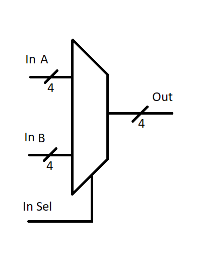
There is another combinational logic device I’d like to quickly introduce you to - it’s called a multiplexer, or mux for short. It has a set of input signals, some select lines, and a single output. Based on the value at the select line inputs, the appropriate input is propagated to the output.
From similar reasoning that we used above, the number of select lines required is equal to where is the number of distinct inputs to be selected between.
A non-traditional looking truth table will summarize this behavior succinctly:
For a mux with data inputs A and B:
| SEL | Out | |
|---|---|---|
| 0 | A | |
| 1 | B |
Perhaps more traditionally for the case where A and B are both 1 bit:
| SEL | A | B | OUT | |
|---|---|---|---|---|
| 0 | 0 | 0 | 0 | |
| 0 | 0 | 1 | 0 | |
| 0 | 1 | 0 | 1 | |
| 0 | 1 | 1 | 1 | |
| 1 | 0 | 0 | 0 | |
| 1 | 0 | 1 | 1 | |
| 1 | 1 | 0 | 0 | |
| 1 | 1 | 1 | 1 |
You could go create this out of individual gates at this point - an exercise which is left up to the user.
Just like we’ve ganged flip-flops together in parallel to make an bit register, you can also gang 1-bit mux’s together to make an bit mux, which is what we’ll need for Earth clock.
The multiplexer is used enough that it gets its own special symbol. Here’s one drawn where A and B are both 4 bits wide.
New Dawn
In particular, when our “new day detection” circuitry indicates that the next second is the start of a new day (and the current time should therefor be 0), we can use that 1-bit output and a mux to switch the value of the input to the registers:
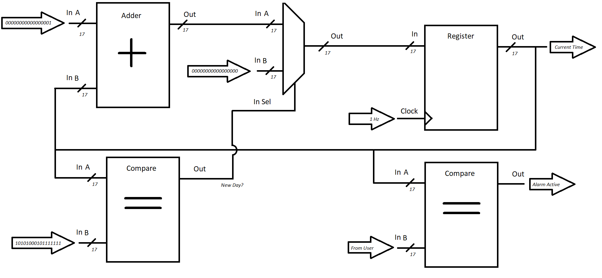
Here, we see that when our “next-day” detection logic indicates the next second should be 0, we pass in a constant value of all-0-bits to the input of the register. In all other cases, we continue to pass the same thing we used to pass - current time + 1.
The alarm circuitry would need very little adjustment - only to increase the total number of input switches used to select the “alarm” time.
And just like that, we’ve constructed a functional earth alarm clock. Good job team!
RAM
While our alarm clock adventures have been fun, it turns most people don’t build their alarm clocks from scratch.. The ones on the market have far more features and it rarely makes sense to build one yourself like we described, unless you want to just have some fun.
Building your own RAM chips is also not recommended for anything except leisure. However, it’s worthwhile going over the basics of what features a piece of Random-Access Memory has to support, and propose one way of going about doing this with the circuits we know about.
Accessing Randomly
Computer Memory is a digital device which stores and recalls large chunks of data. As you may know, and as we already mentioned, RAM is an acronym which stands for “Random Access Memory” - it means that a user of a RAM chip can access any particular part of memory at any time. It also implies that the user can write a new value to any particular part of memory at any time. As a side note, the other common type of memory is called ROM, for “Read Only Memory”. This type can store information, but not change it.
When reading and writing to a RAM chip, the location where things are stored is referred to as an “address”. In general, on a chip, the addresses are just numbered 0, 1, 2, … up through the maximum size of the chip. When you see a chip say it can store 1 MB (megabyte ~= bytes), this refers to the quantity of addresses available for storing data. If each address refers to one byte, the memory is said to be byte addressable and the addresses would go from 0 up through 1048576 or so.
Think of addresses just like the addresses on houses. Each house has a mailbox, and each house has a number on it. When you want to “store” (ie give) data to a certain mailbox, you provide both the “data” (your package or letter) and the address to put it in. A mailman then does the job of storing the data in the right spot. The data remains there till the owner recalls it from the appropriate mailbox. The numbers of the address help coordinate the data going to the right spot, so the right person gets it back out.
Of course, in real RAM, there’s usually no restrictions on who can read or write to each address - unlike in the US, where taking someone else’s mail is a felony. Computers are supposed to be general purpose computation devices, so it’s rare that hardware enforces read/write restrictions based on identity. This sort of security, if required, is usually added by software or specialized processor hardware.
The Prototype RAM Chip
Every RAM chip will have to have a few connections:
- An input for the address from which to read data
- An output which contains the data recalled from the read address
- An input for the address to which to write data
- An input for the data to write at the write address
- A clock to synchronize read/write operations with data input and output.
Depending on what brand and model of RAM chip you have, you may see certain of these functions tied together (ie one address for read/write) or split apart (ie two clocks - one for read and one for write). Some have enable lines to turn on or off read/write functionality as needed. All these features are nice to have, but add cost and increase pin count. So, it’s all just an engineering tradeoff. Pick the RAM chip with all the features you need, and that matches your budget.
When a processor wants to store a value, the process is generally:
- Assert the bits of value onto the data input
- Assert the bits of the address onto the write address input
- Allow the clock cycle to occur.
Reading back a value is very similar:
- Assert the bits of the address onto the read address input
- Allow the clock cycle to occur
- Read the value of the bits on the data output
Note that most RAM chips do not store their value over power cycle. When you remove power from the device, all the data disappears. When you re-apply power, the device reads all 0’s or all 1’s (depends on the underlying technology).
Internals of a Theoretical RAM Chip
I don’t want to get too deep into how to design the internals of the RAM chip. This is because the actual way they are made is highly optimized (some using only a single transistor per bit storage), and it looks very dissimilar from the usual gate logic we think about digital logic in. Still, it is very possible to construct a RAM chip from only the gates and flip-flops we already know about, and is an interesting thought experiment to figure out how to make it happen.
Here’s the highlights of a plausible (abet inefficient) way to do it - I’ll leave the details of the implementation up to the reader to sort out.
- Each address has, at its core, an 8-bit register (same as above) to store the value.
- Every register is fed from the same clock.
- One giant MUX at the output takes the read address input, and selects the proper register to pass to the output
- Each register’s output loops back around to its input through a mux and some digital logic, such that the value usually never changes (output of register fed right back to input).
- However, that input logic is set up such that when the write address input matches that register’s address, the data from the write data input is used instead.
There are some key inefficiencies with this system, however:
- Muxes which select between 1,000,000 inputs are ineffective to make as a single unit. It’s more efficient to split it up into lots of little tiny pieces.
- At scale, gate delays may start to limit clock speed. Having additional buffers to temporarily store the read/write values while the internal circuitry changes state can help mitigate this
- It’s worthwhile noting that in modern processors, RAM is usually asynchronous from and slower than the main processor. This can sometimes be part of the reason extra chips are needed on a motherboard to “drive” the RAM chips, converting data between the domain of the processor and the memory circuits.
- The loop-back circuitry on every register can be eliminated by having two clocks (one for read, one for write), or some set of “enable bit” inputs that the processor controls - writes are commanded only when required.
- The read-mux and write-mux circuitry can sometimes be combined into the inside of the register in an enable/disable fashion.
For more info on “real” RAM chips, search around for “Memory Cell”, like on wikipedia. The key takeaway is that there are a huge number of different ways to implement RAM, but that shouldn’t matter. As far as the processor is concerned, it’s just an abstract device which can store and recall data from little mailboxes we call “addresses”
Next Steps - Where are we going?
With the introduction of combinational circuits like adders and mux’s, and some sequential logic like registers and RAM, we’re now almost ready to start delving into how these are combined together in a traditional processor. We’ll start to cover this in a primer discussion on Processor Architecture.
-
Flaw - or limitation or opportunity. All words could apply, just pick the one that says what you want to say. ↩
-
Or at least, it ought to. Sometimes the marketing department has other ideas. But we still like them, because they help sell the things, which makes money, and lets the engineers make more things, and have food to eat. ↩
-
Turns out, because of gate delay, the ripple-carry adder is actually a bad design for an adder circuit. Think about what happens if you had 1000 stages. How long do you have to wait for the full result to be available? Think about how many gate propagations are needed to calculate the final carry-out signal. Dis nasty. ↩
-
Forgive the odd drawing here - you can ignore the numbers right by the gates. I’m testing out using KiCad for schematic capture and design. It’s a bit cumbersome for these educational purposes, but can draw simple logic diagrams well. Looks super powerful as an electronic schematic and printed circuit board design tool though! I highly recommend it so far! ↩ ↩2